No products in the cart.


Description

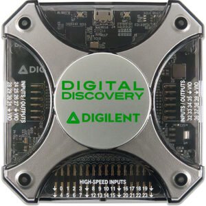
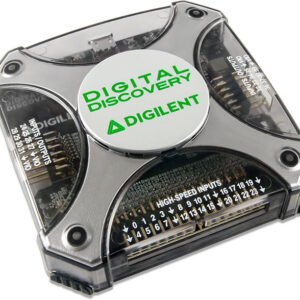
Digilent Digital Discovery
- 16-channel pattern generator (1.2…3.3V CMOS, 100MS/s)
- Two input/output digital trigger signals for linking multiple instruments (1.2…3.3V CMOS)
- 24-channel digital logic analyzer (1.2…3.3V CMOS, up to 800MS/s(with the High Speed Adapter))
Portable Logic Analyzer and Digital Pattern Generator
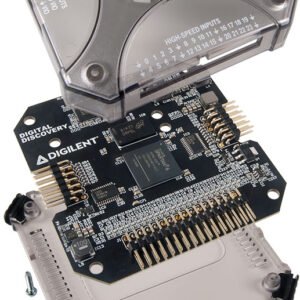
The Digilent Digital Discovery is a combined logic analyzer and pattern generator instrument that was created to be the ultimate embedded development companion. The Digital Discovery was designed to optimize channels, speed, and portability. The small form factor facilitates easy storage and provides a whole suite of advanced features to allow you to debug, visualize, and simulate digital signals for most embedded projects. The digital inputs and outputs can be connected to a circuit using simple wire probes or breadboard wires; alternatively, the Digital Discovery High Speed Adapter and impedance-matched probes can be used to connect and utilize the inputs and outputs for more advanced projects.
The Digital Discovery was designed for anyone embarking on embedded development. Its features and specifications were deliberately chosen to maintain a small and portable form factor, withstand use in a variety of environments, and keep costs down, while balancing the requirements of operating on USB Power.
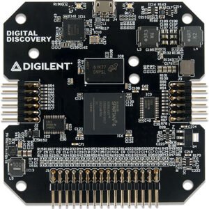
Architectural Overview and Block Diagram
Digital Discovery’s high-level block diagram is presented in Figure 2, below. The core of the Digital Discovery 2 is the Xilinx Spartan-6 FPGA (specifically, the XC6SLX25-2 device). The WaveForms application automatically programs the Discovery’s FPGA at start-up with a configuration file designed to implement a multi-function test and measurement instrument. Once programmed, the FPGA inside the Discovery communicates with the PC-based WaveForms application via a USB 2.0 connection.
The WaveForms software works with the FPGA to control all the functional blocks of the Digital Discovery, including setting parameters, acquiring data, and transferring and storing data into the DDR3 memory. Signals and equations also use certain naming conventions. Signals in the Input block use “DIN” prefix to indicate these are inputs only. Signals in the Input/Output block use “DIO” prefix. Signals at the user connectors include “USR” in their names, while signals at the FPGA pins include “FPGA”. Signals at the FPGA pins driving the pull resistors for DIO signals, include “PULL” in their names. DIN inputs are indexed 0 to 23, DIO input/outputs are indexed 24 to 39.
Product General Attributes | |
|---|---|
| Shipping Weight | 0.50 LBS |
| HTS/Schedule B Number | 8471809000 |
| ECCN Number | 3A992.a |
| Country of Origin | Taiwan |
You must be logged in to post a review.
None
Related products


 Digilent Digital Discovery ...
 $251.90
Our team of knowledgeable professionals is here to help you make informed decisions. Whether you need product recommendations, technical support, or guidance on your purchase, we're just a click away.
Contact Us Now:
📧 sales@nestesinstruments.com
📞 +1 (833) 763-7837
Let us assist you in finding the perfect solution!
Contact Us Now:
📧 sales@nestesinstruments.com
📞 +1 (833) 763-7837
Let us assist you in finding the perfect solution!
Reviews
There are no reviews yet.