No products in the cart.
Need help? Call us:
+1 (833) 763-7837
Menu
Categories
- Accessories
- Air Purification Accessories
- Antennas
- Attenuators
- Barcode Scanners
- Batteries and Chargers
- Bottles and Dispensers
- Cables - Misc
- Carrying Straps, Lanyards and Harnesses
- Carts
- Case and Cart Accessories
- Cases
- Cathodic Protection Accessories
- Coaxial
- Crimper Accessories
- Datacom Accessories
- Dry Block Bath Inserts
- EMI Accessories
- Enclosure Accessories
- FIber Optic Accessories
- Fiber Optic Cables
- Gas Detection Accessories
- General Accessories
- GPIB Adapters
- Heating Elements
- Hipot Accessories
- Hoses - Miscellaneous
- HVAC Accessories
- Induction Heater Accessories
- Input Cards
- Jacks /Adapters /Plugs /Clips /Terminators/Coaxial
- Jobsite Storage and Cabinets
- Knockout Accessories
- Lab Accessories
- LCR Test Fixtures
- LED and LCD Displays
- Manuals
- Material Handling Accessories
- Microphones
- Microscope Accessories
- Motors
- Options
- Pinhole/Holiday Detector Accessories
- Plumbing Accessories
- Precision Measuring Instrument Accessories
- Pressure Calibrator Modules
- Printers and Printing Supplies
- Probes
- Rack Mounts and Stands
- Repair Parts and Fuses
- Scale Accessories
- Shunts
- Software
- Soldering Accessories
- Spectrum Analyzer Accessories
- Static Control Accessories
- Switch and Semiconductor Modules/Access
- Test Fixtures
- Test Leads and Instrument Accessory Kits
- Thermal Imager Accessories
- Training and Education
- Underground Utility Location Accessories
- Vibration Accessories
- Video Accessories
- Voltage Transformer
- Warranty and Calibration
- Amplifiers / Preamps / Preamplifiers
- Audio Equipment
- Automotive Test Tools
- Battery Testing
- Blower Door and Duct Testing
- Borescopes / Boroscopes
- Clamp Meters
- Cleanroom
- Color and Appearance
- Conduit Benders
- Current Sensors
- Datacom and Networking Products
- Dataloggers Data Acquisition
- Decade Boxes
- Distance Meter
- Electrical Parts and Products
- Cable and Wire
- Cable Reels
- Electrical Cord
- Electrical Jumpers and Pigtails
- Electrical Parts
- Electrical Plugs and Connectors
- Line Splitters
- Lockout / Tagout
- Outlet Boxes
- Pulling Products
- Pushbutton Pendant Stations
- Receptacle Testers
- Temporary Power Distribution
- Terminal Blocks and Strips
- Terminals and Crimps
- Wall Plates
- Wire Management
- Wire Ties
- Work Lighting and String Lighting
- Enclosures and Boxes
- Environmental Testers / Physical Property
- Anemometer / Air Flow
- Barometers and Altimeters
- Chlorine Tester
- Dissolved Oxygen Meter / Fluoride
- EMF / ELF Meter
- Heat Index Monitors
- Humidity Meters
- Hygrometers
- Moisture Meters
- Nuclear Radiation Monitors
- PH / ORP Meters
- Psychrometer
- Refractometers / BRIX
- Scales / Weight
- Sound Level Meters
- Stopwatches / Timers / Clocks
- Water Quality Accessories
- Water Quality Meters
- Weather Measurement
- Wind Tunnels
- Flow Measurement
- Force / Torque / Hardness Meters
- Gas Detection
- Ground Testers
- Health and Safety
- HVAC Equipment and Instruments
- Automotive RRR Machines
- Brazing
- Combustion Analyzers
- Hose Adapters, Valves and Parts
- HVAC - Testing - Adjusting - Balancing
- HVAC Equipment - Misc
- HVAC Manifolds and Gauges
- HVAC Vacuum Pumps
- Refrigerant Leak Detectors
- Refrigerant Recovery Machines
- Refrigerant Recovery Tanks
- Smoke Pump Test Kits
- Tubing Tools
- Vacuum Gauges
- Hydraulic Cylinders
- Indoor Air Quality
- LCR Meters / Impedance Measurement Products
- Leakage Detectors
- Life Sciences Equipment
- Autoclaves and Sterilization
- Bunsen Burners
- Centrifuges
- Cold Storage
- Colony Counters
- Dry Block Heaters and Cooling Blocks
- Environmental Test Chambers
- Flame Photometers
- Flocculators
- Fluidized Bed Baths
- Gel Imaging Electrophoresis
- Glassware Washers-Dryers
- Heating Mantles / Electromantles
- Homogenizers
- Incubators
- Kjeldahl Apparatus
- Lab Apparatus - Misc
- Laboratory Ovens
- Laboratory Pumps
- Laboratory Water Purification Systems
- Magnetic Bead Based Purification
- Melting Point Apparatus
- Mixers Rotators and Stirrers
- Pipettes
- Reaction Station
- Recirculating Chillers / Coolers
- Refrigerated Heating Circulators
- Rotary Evaporators
- Shakers and Rockers
- Slide Warmers
- Spectrophotometer
- Thermal Cycler / PCR
- Titrators
- Water Baths and Liquid Baths
- Logic Analyzers
- Materials Testing
- Megohmmeter / Insulation Resistance Testers
- Micro-Ohmmeter / Milliohmmeter
- Microscopes
- Multimeters
- Network Analyzer
- Oscilloscopes
- Panel Meters
- Personal Protective Equipment
- Phase / Motor / Transformer Testing
- Power Measurement
- Power Supplies
- Process / Calibration
- Programmers / IC and RAM Testers
- Protocol Analyzers
- Prototyping
- Radiometric
- Reliability / Preventative Maint / Rotational
- RF, Microwave, EMI
- Safety Testing / Surge Testing
- Signal Generators / Counters
- Signal Level Meters - CATV / CCTV / Satellite
- Solar Analyzers
- Soldering Equipment
- BGA Rework Station
- Chemicals
- Cleaning Pins and Drills
- Depaneling Systems
- Desoldering Equipment/Rework Stations
- Desoldering Irons
- Dispensing Equipment
- Flux
- Flux Remover
- Fume Extraction
- Hot Air Guns
- Hot Air Pencils
- Lead Forming Equipment
- Nitrogen Generation
- Nozzles
- PCB Supports and Holders
- Pre-Heater
- Solder
- Solder Wick
- Soldering Equipment
- Soldering Irons
- Soldering Pots
- Soldering Robots
- Soldering Stands
- Soldering Stations
- Soldering Tip Cleaners
- Soldering Tip Thermometers
- Soldering Tweezers
- Sponges and Brass Wool
- Thermal Wire Strippers
- Tips
- Vacuum Pick-Up Tools
- Sporting / Hunting / Law Enforcement Optics
- Static Control
- Surveying / Construction Measurement
- Thermal Imagers
- Thermometers
- Thickness Gauges
- Tools
- Blackeners
- Cable Cutters
- Cable Strippers
- Cable Tie Guns
- Combination Squares
- Conduit Tools
- Crimpers
- Cutters
- Cutting Tools
- Datacom / Fiber Optic Tools
- Drill Bits and Sets
- Drill Rod
- Dry Lubricants
- Electric Screwdrivers
- Feeler Gage
- Fiber Optic Cable Tools and Fiber Scopes
- Flashlights and Headlights
- Ground Flat Stock
- Hex Drivers, Torx Drivers
- Hose Benders
- Hose Clamps
- Hot Melt
- HVAC Service Tools
- Insulated Tools
- Keystock
- Knockout Tools
- Layout Fluid
- Level Measurement
- Maintenance Kits
- Multi-Tools
- Other Hand Tools
- Pliers
- Pneumatic Hand Tool Operators
- Power Tools
- Probes & Scribes
- Punch & Die Sets
- Punchdown Tools
- Remote Hydraulic Pumps
- Screwdrivers
- Shims & Shim Stock
- Sockets & Ratchets
- Spatulas
- Telecom Service Tools
- Telescopic Tools
- Threaded Rod
- Tool Kits
- Tool Wrap
- Tweezers
- Vises
- Wire
- Wire Strippers
- Wrenches & Wrench Sets
- Toys / Cool Stuff
- Transmission Line/Station Testing
- Cable Testing
- Circuit Breaker Testers
- Corona Detection
- Dielectric Oil Testing
- High Current Detectors / Indicators
- High Voltage Detectors / Indicators
- Hot Sticks
- Phasing Sticks
- Primary Injection Test Equipment
- Safety Equipment
- Secondary Injection Test Equipment
- SF6 Gas Leak Detectors
- Transformer Testing/TTR
- Transmission Cable Height Meters
- Video Distribution Equipment
- Video Test Equipment
- Voltage / Continuity and Non-Contact Testers
- Wire Tracers / Circuit Breaker Tracers
- Workbenches
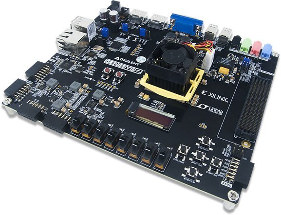
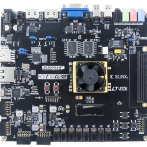
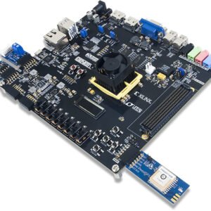
Digilent Genesys2 – Kintex-7 FPGA Development Board
Brand:
33 people are viewing this product right now
$1,208.90
Shipping calculated at checkout.
Estimated delivery:5 days
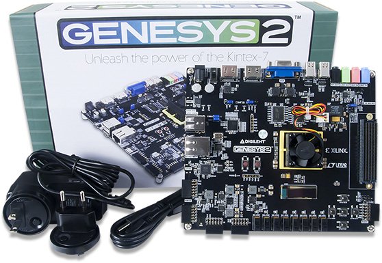
Genesys II Product Kit
- 50,950 logic slices (from Genesys up 7x), each with four 6-input LUTs and 8 flip-flops
- Close to 16 Mbits of fast block RAM (up 7x)
- Ten clock management tiles, each with phase-locked loop (PLL)
- 840 DSP slices (up 17x)
- Internal clock speeds exceeding 450MHz
- On-chip analog-to-digital converter (XADC)
- Up to 10.3125Gbps gigabit transceivers
- 1800Mbps DDR3 data rate with 32-bit data width
- Commercial -2 speed grade
- Fully bonded 400-pin FMC HPC connector
Have any Questions?
Feel free to Get in touch
Guarantee Safe and Secure Payment Checkout
Description

Digilent Genesys2
- Digilent Adept USB port for programming and data
- Ten GTX lanes available in the FMC connector
- Micro SD card connector
- Audio codec w/ four 3.5mm jacks
- Serial Flash
Kintex-7 FPGA Development Board
Powered by Xilinx’s Virtex-7 XC7V690T FPGA, the NetFPGA-SUME is an ideal platform for high-performance and high-density networking design. 32 GTH serial transceivers have been used to provide access to 8 lanes of end-point PCI-E (Gen3 x8), 4 SFP+ (10Gbps) ports, 2 SATA-III ports (6Gbps), and 18 data-rate-adjustable GTH ports through an HPC-FMC connector and a QTH connector. Wide high-speed memory interfaces in the form of three 72 MBit QDRII+ SRAMs with 36-bit buses and two 4GB DDR3 SODIMMs with 64-bit buses provide an ideal memory solution for common networking applications.
Power Supplies
The Genesys 2 board can receive power from an external power supply through the center-positive barrel jack (J27). The external supply voltage must be 12 V ±5 %. The Genesys 2 cannot be powered from the USB bus. All Genesys 2 power supplies can be turned on and off together by a single logic-level power switch (SW8). Power supplies are either enabled/disabled directly by the power switch or indirectly by other supplies upstream. A power-good LED (LD15), driven by the “power good” output of the on-board regulators, indicates that the supplies are turned on and operating normally. An overview of the Genesys 2 power circuit is shown in the left figure.

Power Monitoring
The configuration and calibration registers are volatile, so they need to be initialized after power-up. After initialization is done voltage, current, and power values can be read from dedicated registers. It is recommended to add glitch filters to the I2C master controller to avoid spurious start or stop conditions occurring on the bus. This is especially important when using an external I2C master connected to the J18 header (not mounted by default).

FPGA Configuration
After power-on, the Kintex-7 FPGA must be configured (or programmed) before it can perform any functions. You can configure the FPGA in one of four ways:
- A PC can use the Digilent USB-JTAG circuitry (port J17, labeled “USB JTAG”) to program the FPGA any time the power is on.
- A file stored in the nonvolatile serial (SPI) flash device can be transferred to the FPGA.
- A programming file can be transferred to the FPGA from a micro SD card.
- A programming file can be transferred from a USB mass-storage device (ex. pen drive) attached to the USB HOST port.

Memory
The Genesys 2 board contains two external memories: a 1GiByte volatile DDR3 memory and a 32MiByte nonvolatile serial Flash device. The DDR3 uses two 16-bit wide memory components with an industry-standard interface soldered on the board resulting in a 32-bit data bus. The serial Flash is on a dedicated quad-mode (x4) SPI bus.
Ethernet PHY
The Genesys 2 board includes a Realtek RTL8211E-VL PHY paired with an RJ-45 Ethernet jack with integrated magnetics to implement a 10/100/1000 Ethernet port for network connection. The PHY interfaces with the FPGA via RGMII for data and MDIO for management. Bank 33 powered at 1.5V is populated with these signals. The auxiliary interrupt (INTB), power management (PMEB) signals are wired to bank 32 and powered at 1.8V. Both of these signals are open-drain outputs from the PHY and need internal pull-ups enabled in the FPGA, if they are used.
At power-on reset, the PHY is set to the following defaults using the configuration pins in parenthesis:
- Auto-negotiation enabled, advertising all 10/100/1000 modes (AN[1:0])
- PHY address=00001 (PHY_AD[2:0])
- No delay for TXD and RXD relative to TXC and RXC for data latching (RXDLY, TXDLY)
If an Ethernet cable is plugged in, establishing a link is attempted straight after power-up, even if the FPGA is not programmed.
Two status indicator LEDs are on-board near the RJ-45 connector that indicates traffic (LD10) and valid link-state (LD9). The table below shows the default behavior.
USB UART Bridge(Serial Port)
The Genesys 2 includes an FTDI FT232R USB-UART bridge (attached to connector J15) that lets you use PC applications to communicate with the board using standard Windows COM port commands. Free USB-COM port drivers, available from Windows Update or www.ftdichip.com under the “Virtual Com Port” or VCP heading, convert USB packets to UART/serial port data. Serial port data is exchanged with the FPGA using a two-wire serial port (TXD/RXD) with no handshake signals. After the drivers are installed, I/O commands can be used from the PC directed to the COM port to produce serial data traffic on the Y20 and Y23 FPGA pins.

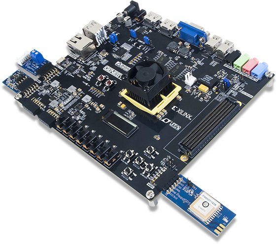
Pmod Connectors
The Pmod connectors are arranged in 2×6 right-angle, 100-mil female connectors that mate with standard 2×6 pin headers. Each 12-pin Pmod connector provides two power pins (6 and 12), two ground pins (5 and 11), and eight logic signals, as shown in Fig. 20. The VCC and Ground pins of can deliver up to 1A of current per pin. Pin assignments for the Pmod I/O connected to the FPGA are shown in.

None
Be the first to review “Digilent Genesys2 – Kintex-7 FPGA Development Board”
You must be logged in to post a review.
Manuals/Guides
ManualsOther
Related products
Our team of knowledgeable professionals is here to help you make informed decisions. Whether you need product recommendations, technical support, or guidance on your purchase, we're just a click away.
Contact Us Now:
📧 sales@nestesinstruments.com
📞 +1 (833) 763-7837
Let us assist you in finding the perfect solution!
Contact Us Now:
📧 sales@nestesinstruments.com
📞 +1 (833) 763-7837
Let us assist you in finding the perfect solution!








Reviews
There are no reviews yet.